Quantcast
Channel: Amplifiers
Viewing all 68573 articles
Browse latest View live

Forum Post: RE: Difference Amplifier: Input Offset Voltage

$
0
0

Bonnie,

I am using 0-5V power ( from a bench supply, also tested with 6V-SMPS through 5V V-REGULATOR).

I wanted to omit the offset circuitry to simplify the calibration for others.  The reference is ground.  

The thermocouple range needs to be up to 1100 C.  This makes voltage swing from 0 to 3.3 V on the output and

  0 to 47 mV  on the input.  

NOTE: With a 50K resistor connected to neg terminal of the thermocouple 100ohm input reistors and 150nF(poly) , 2 X 10nF from teminals to

 ground I was getting an offset of 0.4mV.  This is well bellow the max error.(that would be acceptable).

This is the setup shown in the data sheet for thermocouple design.


Forum Post: RE: AC amplification problem - coupling capacitor isn't blocking DC from electret mic - using TL071

$
0
0

Thank you very much! I appreciate your help and will follow your advice :)

David.

Forum Post: RE: I want to amplify a low frequency and low amplitude signal and am facing the problem of noise and offset.

$
0
0

Hello Dinesh,

I believe you should evaluate the INA333 for this application. That said, please understand that we are not authorities on acquiring biomedical signals. Most of our experience is with ECG...perhaps you will find the following E2E Wiki useful:

http://e2e.ti.com/support/amplifiers/precision_amplifiers/w/design_notes/2437.ecg-heart-signal-acquisition.aspx

I also suggest searching the E2E forums for there may be other threads that provide greater detail of acquiring EMG signals.

We would greatly appreciate it if you could follow up with how you designed your project because EMG is a popular topic. We and other forum readers would find such information very useful!

Forum Post: RE: Transimpedance Amplifier problem

$
0
0

Thanks John,


But I have even used that circuit before, but with a smaller feedback resistor. I think I would have problems with leakage currents if I were to put it on the board, since my feedback resistor is so big. If it weren't for that I think I would be okay, since I have a DAC providing an offset current which could be used to dial out the Igs current of a few pA.


Regards,

Jim Gannon

Forum Post: RE: ACF2101 Switched Integrator, HOLD pin not functioning in TINA simulation

$
0
0

T.M.,

There is nothing wrong with the switches in the ACF2101 macro model. I think that your input source is causing the problem. If you place a voltage probe on SwIn you will discover that, when in hold, the voltage will go to approximately 10 volts. This is well above the positive supply voltage and the ACF2010 model is not operating correctly. You are overdriving the switch. You can reduce the impact of this problem by placing parrallel diodes across the current source. When that is done you will see that the voltage across the current source is limited to +/- 6 mV. You will also see the hold function working properly.  

In terms of the actual device, if you place a photodiode on the front end this phenomena will not happen. The device will work properly.

Forum Post: TAS5717 Audio Amplifier not outputting. Possible problem with registers?

$
0
0

Hello,

Via I2C, I am setting the registers in the TAS5717 (slave) from a LM3S9B96 (master) micro-controller.

These are the values I am setting:

 (the first hex number is the register I am writing to, and all the consecutive hex numbers are the values I am writing to that register) 

"X1B 82",
"X03 80",
"X11 77",
"X12 7F",
"X13 77",
"X14 7F",
"X1C 07",
"X05 00",
"X0E F1",
"X00 60",
"X04 05",//
"X0A 00 C0",
"X07 00 00",
"X50 0F 70 80 10",
"X25 01 02 13 45",
"X70 00 80 00 00",
"X71 00 00 00 00",
"X74 00 80 00 00",
"X75 00 00 00 00",
"X46 00 00 00 21",
"X43 00 74 00 00",
"X56 00 80 00 00",
"X57 00 02 00 00",
"X40 08 00 00 00",
"X73 00 80 00 00",
"X72 00 00 00 00",
"X76 00 66 66 66",
"X77 00 80 00 00",
"X4F 00 00 00 06",
"X3B 00 08 00 00 00 78 00 00",
"X3C 00 00 01 00 FF FF FF 00",
"X3E 00 20 00 00 00 40 00 00",
"X3F 00 08 00 00 FF F8 00 00",
"X51 00 80 00 00 00 00 00 00",
"X52 00 80 00 00 00 00 00 00",
"X58 00 80 00 00 00 00 00 00 00 00 00 00 00 00 00 00 00 00 00 00",
"X59 00 80 00 00 00 00 00 00 00 00 00 00 00 00 00 00 00 00 00 00",
"X5A 00 80 00 00 00 00 00 00 00 00 00 00 00 00 00 00 00 00 00 00",
"X5B 00 80 00 00 00 00 00 00 00 00 00 00 00 00 00 00 00 00 00 00",
"X26 00 80 00 00 00 00 00 00 00 00 00 00 00 00 00 00 00 00 00 00",
"X30 00 80 00 00 00 00 00 00 00 00 00 00 00 00 00 00 00 00 00 00",

"X27 00 7F 71 CA 0F 01 1C 6B 00 7F 71 CA 00 FE D2 1C 0F 81 0A F2",
"X28 00 7E 23 7F 0F 06 4E 40 00 7C 17 68 00 F9 B1 C0 0F 85 C5 18",
"X29 00 7F 77 F6 0F 07 50 35 00 7B 5D 2F 00 F8 AF CB 0F 85 2A DB",
"X2A 00 7C D5 0F 0F 35 15 81 00 6D 79 96 00 CA EA 7F 0F 95 B1 5A",
"X2B 00 DC 3F 74 0F 3B 93 F4 00 45 90 CF 00 3D E6 A7 0F E4 B5 22",
"X2C 00 80 00 00 00 00 00 00 00 00 00 00 00 00 00 00 00 00 00 00",
"X2D 00 80 00 00 00 00 00 00 00 00 00 00 00 00 00 00 00 00 00 00",
"X2E 00 80 00 00 00 00 00 00 00 00 00 00 00 00 00 00 00 00 00 00",
"X2F 00 80 00 00 00 00 00 00 00 00 00 00 00 00 00 00 00 00 00 00",

"X31 00 7F 71 CA 0F 01 1C 6B 00 7F 71 CA 00 FE D2 1C 0F 81 0A F2",
"X32 00 7E 23 7F 0F 06 4E 40 00 7C 17 68 00 F9 B1 C0 0F 85 C5 18",
"X33 00 7F 77 F6 0F 07 50 35 00 7B 5D 2F 00 F8 AF CB 0F 85 2A DB",
"X34 00 7C D5 0F 0F 35 15 81 00 6D 79 96 00 CA EA 7F 0F 95 B1 5A",
"X35 00 DC 3F 74 0F 3B 93 F4 00 45 90 CF 00 3D E6 A7 0F E4 B5 22",
"X36 00 80 00 00 00 00 00 00 00 00 00 00 00 00 00 00 00 00 00 00",
"X37 00 80 00 00 00 00 00 00 00 00 00 00 00 00 00 00 00 00 00 00",
"X38 00 80 00 00 00 00 00 00 00 00 00 00 00 00 00 00 00 00 00 00",
"X39 00 80 00 00 00 00 00 00 00 00 00 00 00 00 00 00 00 00 00 00"

However, when I read the registers, I can see all the values that I wrote except for the 5th and 17th value (which both happen to be 0x0F) of registers 0x27 to 0x2B and 0x31 to 0x35. When I read these positions in the resisters, I see "0x03" instead of "0x0F.

Ontop of all this, I am still not getting any output from the TAS5717 Audio Amplifier. Am I missing any registers? Or am I placing the wrong value into a register?

Any help/input would be most appreciated (:

Forum Post: RE: THS4631 conversion issue

$
0
0

Hi Roy,

Yes. You are correct. The differential OPAMP output should be independent of the common mode voltage of the differential OPAMP.  But, the way of looking at the differential OPAMP output is incorrect. You are actually looking at the V(p-p) of two different signals and adding them up.

You should see the V(p-p) difference for the ADC_input+ in the schematic and add that with the V(p-p) difference for the ADC_input- in the schematic. This comes out to be 55mV for both the current direction cases.

Thanks,

Rohit


Forum Post: TAS5548EVM - device configuration on powerdown/powerup

$
0
0

I started using my new TAS5548EVM with the PPC software last night, with headphones connected to the headphone output. 

All works well, shutting down the PPC software does not affect operation of the EVM. 

However, disconnecting/reconnecting the USB cable to the EVM (effective powerdown/powerup) seems to put the EVM into a MUTE state (observed: no output via headphone port) which I can only clear by starting up the PPC software again.  The biquad setting have been overwritten and I must reload them again.

The datasheet for the TAS5548 (Section 5.2.2) states "The TAS5548 is placed in the reset mode either by the power-up reset circuitry when power is applied, or by setting the RESET terminal low."

What I would like to do is have the TAS5548 retain its status, settings, volume/routing/biquads etc (all I2C registers) upon powerdown/powerup, or automatically return to its status prior to powerdown, without commands via the USB port.

I can see that the EVM uses the TAS1020B for I2C commands, and that there is an EEPROM on board.  I have no experience with I2C/microcontroller programming...

What do you suggest?

Many thanks,

Mike


Forum Post: RE: LM7171: using a unipolar power supply?

$
0
0

Hello again,

Prototyping boards with high speed amplifiers like the LM7171 don't work well at all, as you have already noted. You may be able to get an EVAL board and try using that instead. Also, large value resistors tend to not work well either (due to parasitic capacitance roll-off effects).

If you let me know the package you are using for the LM7171, I might be able to point you to some EVAL boards that you can acquire at www.ti.com and use for testing.

Please let me know.

Regards,

Hooman

Forum Post: RE: THS4631 conversion issue

$
0
0

Hi Roy,

As far as the spikes in the outputs are concerned, that is because of the mismatch in the clock signal rise time at the difference amplifier (THS4631) input.  This spike is only amplified at the fully differential OP_AMP (THS4520). Also, in real world scenario, there could be mismatch in phases between the buffers OPA659 which would only worsen the spikes. Is there a specific reason why you are using a clock signal (square wave) instead of a sine wave? Square wave when sampled at the ADC input will demonstrate more spurious spectrum rather than a sine wave.

Regards,

Rohit


Forum Post: RE: INA333 problem. Output goes to zero when i bias input.

$
0
0

Thank you for your reply. I actually found out that by removing the IC from my PCB design, which contains a lot more than just this amplifier, and mocking up a simple test with only the IC and the right resistors, the output works, so i think i may have some problem with my PCB layout that I will have to figure out.

The most important thing i would like to know here was weather or not the high resistor bias circuits on the inputs would somehow be a problem regarding the amplifiers bias current return path?

With respect to the reference pin i also read the part of buffering but for this preliminary test i just use the diode or maybe a simple resistor divider. For my final design i will go for the buffered reference. I just need to be sure that feeding this reference with a high impedance source didn't cause my problem?

Below you will see the circuit with the measuring part present:

So the input signal is actually a transformed signal which needs to be pulled up to a DC level where the lower part is not clipped, hence the bias circuit. I had also at the beginning thought about some kind of bias circuit but my problem, as i also stated before, is the Q factor in the resonance circuit L8 C15. It seems unavoidable that the DC circuits will become the dominant resistive part of this factor and therefore it needs to be as high as possible.

By using 100k resistor the system works ok, but of course if you have any recommendations regarding more precise DC bias circuits or IC's please let me know. I'm currently using low ppm high precision resistors on the input which keeps them somewhat close in voltage and since I expect to use no more than 10 times amplification on the INA333 the error is containable, but of course it would be nice with a more elegant solution.

Forum Post: Amplifier parameters Bias current Offset current and Offset Voltage

$
0
0

What is the meaning of Bias current  Offset current and Offset Voltage?

How does the parameters impact application when using amplifier in Noninverting Operational amplifier and Inverting Operational amplifier.

Forum Post: RE: LM4675 Inrush Current & Stability Time

$
0
0

Hi Naokawa-san,

We have obtained the informations of the evaluation and simulation from our customers.
We remade the evaluation schematic, made the simulation schematic.
The evaluation schematic is as follow.


We modified the connection of full differential input and the value of output capacitors.
Our customers are estimating the parasitic inductor value.
The device that is connected output load is the structure like as the small speaker.
This parasitic inductor value would be small.
This device is something we do not know.


On the other hand, The simulation schematic is as follow.


The inrush current flows the output capacitor in this simulation, regardless of output load.


How do you think about the inrush current and the stability time?
Could you please advise to us?

Best Regards,
Kato

Forum Post: Current flowing out of INA226 VIN- terminal when shunt voltage well exceeds 81.92mV

$
0
0

Hello,

  For clarifying the issue, I used INA226EVM to recreate the case.

  VIN- is connected to GND through 6.8k resistor.

  VIN+ is connected to VS(3.32V). See the attached pics for detail setup.

  The multimeter measured voltage drop across (VIN-, GND) is 1.62V. My question is: as VIN- is pulled down to GND by 6.8k resistor and VIN- input impedance is high, why isn't VIN- pulled close to GND?? How comes the 1.62V? Does leakage current as high as 1.62/6.8k = 238uA really flow out of VIN-?

  Thanks in advance!

Forum Post: INA118 SNR Deterioration of the Instrumentation Amplifier

$
0
0

Hi,

We have obtained one question from our customers.
Our customers will use the INA118 as the AD Driver for the ADS7263.
Although we think that the SNR will be changed in relation to cut-off frequency, gain settings, etc., we would like to calculate the SNR of this device.
Could you please tell us how to calculate or SNR values that you calculated or how to calculate by using the TINA-TI or send us the application notes as soon as possible?
There is no problem if the accuracy of the device is more than 14bit.
Could you please advise to us about it.

Best Regards,
Kato


Forum Post: RE: ACF2101 Switched Integrator, HOLD pin not functioning in TINA simulation

$
0
0

Hi B.B,

I'm not seeing the phenomenon you describe so I would like to make sure I understand correctly and that we are using the same circuit and model for the ACF2101. When I run a transient simulation of the schematic I provided using Tina 9.3.50.40 I find the voltage between SwitchIn and GND (using the volt meter named Vswin or a probe on the output pin of the current source) to be 475.57mV max, not the 10V you find.

Could you perhaps provide me with the circuit you are using so I can compare the two and figure out why we are measuring different values.

To further investigate I made sure the initialization demand for the model (HOLD and RESET should be equal to com) is still valid (it is). I have also investigated if the switch times where to long (changed from 5V/1ms to 5V/1us) and changed some of the switch times to make sure the HOLD, RESET and SELECT switches do not change at the same time. None of the changes has any effect on the circuit behaviour.

P.S. I have updated the schematic I use and added the ACF2101 sub-circuit to the attached zip file to make sure we are using the same code.

Forum Post: RE: Inquiry regarding IOUT – Duty cycle characteristic on ULN2803A

$
0
0

Atsushi,

These two devices are the same for all practical purposes. The Toshiba device just has more views of the same performance.

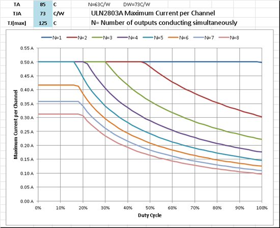
I made de-rating curves for typical VOL performance. Here is "N" original DIP package (Ta = 85C)

 Here is "DW" wide SOIC package (Ta = 85C)

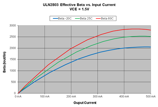
Here is a beta plot I found.


Forum Post: RE: I want to amplify a low frequency and low amplitude signal and am facing the problem of noise and offset.

$
0
0

Hello Dinesh,

With a 5V single supply the common-mode input range fo the INA333 is from 100mV to 4.9V. The output range, however, depends on the common mode signal. Please refer to Figure 21 in the data sheet. From what I understand of ECG, the body is generally biased to 2.5V (which is the common mode voltage) using a right-leg drive circuit (RLD). This is shown in Figure 36. I'm not very familiar with EMG, however. If there is no reference electrode such as the RLD then perhaps you'd be more interested in the INA326. The INA326 has a unique topology for an instrumentation amplifier. This topology allows for beyond rail-to-rail input swing and rail-to-rail output swing without limitation by the input common-mode voltage.  

Forum Post: RE: Op Amp "Automotive Grade"

$
0
0

Hi Josh Batista. If this is going to be your circuit I don't think that it will work because the Wheatstone bridge has been coupled to the input of a differential amplifier which posses some input impedance which is not very high to neglect. Otherwise it will change the balancing point of the bridge. In order to expect the Wheatstone bridge to work in the way that you are expecting, Try instrumentation amplifier here: http://www.ti.com/lsds/ti/amplifiers-linear/instrumentation-amplifier-products.pagedual 

Forum Post: RE: LM7171: using a unipolar power supply?

$
0
0

Hi Aaron,

The dotted RC on the non-inverting input will "low pass filter" your input and will lower the measured frequency response. So, for bandwidth testing, you may want to eliminate the shunt cap or at most use it only for compensation as shown in Figure 57.

What is the capacitance of the load you are trying to drive? Figure 39 shows that you can expect some peaking when driving a capacitive load of 50pF or more, directly. Figure 61 describes the method of isolating the cap load using a series resistance. Apart from board parasitics (which the EVAL board I mentioned may alleviate), I don't have any other ideas as to why you are only getting 200kHz small signal bandwidth when you should be getting close to 20MHz! Try removing your load for now and testing with a 50ohm series output resistor feeding a 50ohm coax cable terminated in 50ohm inside a scope to see if that ups your response reading or not? If the bandwidth limitation is from your load, at least we will know how to tackle this issue.

Let me know and I'll see if I can be helpful.

Regards,

Hooman

Viewing all 68573 articles
Browse latest View live


<script src="https://jsc.adskeeper.com/r/s/rssing.com.1596347.js" async> </script>