Thanks Don. I still have a question about this application. I have a single power supply (24V battery) powering both my preamp and the TPA3130 amp. My preamp circuit is a TL071 op amp using a single supply (+12V off a V regulator), non-inverting, biased with a zener at ~Vs/2. As one side of the output of the preamp/input to the 3130 is GND, how do I insert a TVS diode into this circuit?
↧
Forum Post: RE: TPA3130D2 used for MONO with minimal circuitry for underwater use
↧
Forum Post: RE: HELP PLEASE Strange problem with latest batch of LMC7211
HI Paul,
Many thanks for your speedy reply and suggestions.
I tried so many things to tame the new circuit I forget what I did. I know I decoupled R10 with a large cap and I scrutinised the supply rails for any sign of the fast spikes. I am not sure which manufacturer the latest LMC7211's were from as I just ordered them via Farnell but I can check back on the packaging for the order code and cross ref it back to their website. Don't know about date codes on the bottom as I don't wish to cannibalise the working one (it has COOB) on the top BTW) and I destroyed all but my last problematic sample which is still on my test board - playing up.
The +/- 3.6V is generated from a 9V battery through an ADP3331 High accuracy LDO down to 7.2V. (7.4V being the 'exhausted' point according to Duracell for their PP3) This device also flags 'battery low' on my gadget. The 7.2V is then passed to an artificial 0V generator using a TLE2071 to generate the split rails of +/- 3.6V. All rails are copiously decoupled and I definitely tried many sizes of capacitor directly across the LMC7211. Can't remember if I disconnected the LED....something to easy to try though!
Shoot through sounds like a possible culprit, so I will try all your suggestions and report back.
I can live perfectly with the TL071, but it's driving me mad, why having had two original 'sample' LMC7211's work perfectly, now I bought some, they all play up...sod's law I guess?
Thanks...Dave
↧
↧
Forum Post: RE: INA321 multiplexing
Hi Chris,
Welcome to the e2e forum! The main issue I see with multiplexing the power for each INA321 is that the output pin of the device has an ESD diode to each of the power supply rails, here is a simplified schematic:

Therefore, if the VDD line is pulled to ground on the "disabled" device, then the voltage at the output will be clamped to within 1 diode drop in either direction (positive or negative) from ground. This is not the case with the device is simply in shutdown mode, because both diodes remain reverse biased as long as the signal range is within the supply voltages.
↧
Forum Post: RE: output impedance of LPV521 follower
thank you for your fast response and clear explain.
↧
Forum Post: RE: LMH6624 High gain trans-impedance noise
Hello again Karel,
For your 1st stage: Since the LMH6624 is stable for closed loop gains of 10V/V or higher, I believe your compensation capacitor (C3, capacitor across feedback resistor of 2.2kohm) may have to be raised lowered. You may be experiencing higher noise than expected if your frequency response is peaking due to lack of phase margin.
Looking at Figure 64 from LMH6629 (shown below), if CF (C3 in your case) is too large, your Noise Gain plot will intercept the Open Loop Gain plot at a low y-axis value. For the LMH6624, this intercept should be higher than 20dB (or 10V/V). So, assuming 5pF for your Cin (3pF + other parasitic capacitances), CF < = 0.56pF (vs. 1.2pF that you have shown).
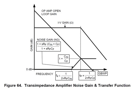
If your CF is too low, however, "fp" would shift right and you may have instability for a different reason.
So, I recommend you lower CF (C3 in your case) and retry the noise test.
Regards,
Hooman
↧
↧
Forum Post: RE: voltage to current converter
Here is another discussion related to current sources:
http://e2e.ti.com/support/amplifiers/etc_amplifiers__other_linear/f/18/p/278637/977535.aspx#977535
Regards,
Hooman
↧
Forum Post: RE: There is someting wrong with application note sbfa005 about UAF42
Hi Robert,
I am glad to see you found the original FilterPro software that has the UAF42 filter synthesis capability.
The bandwidth of the band-pass filter is very narrow, 2 Hz. We can see from the software screenshot that the Q of each stage is 42.2 which is very high. Ringing in an analog filter follows the Q; the higher it is the more sustained the ringing will be when an impulse applied to the filter input. I expect that lowering the Q would help reduce the ringing. Filters are often designed primarily for their frequency response, and their phase and time responses may suffer as a result.
When we look at the number of loops in the filter it doesn't surprise me that it takes upwards to a half second for the amplitude to stabilize. Especially when considering the ringing in the circuit. I simulated the filter using ideal operational amplifiers and the amplitude stabilization time was about the same as using the OPA131 amplifiers. A high Q circuit can be sensitive to an environmental condition such as temperature. That may be what you are observing when you mention susceptibility to environment.
Regards, Thomas
PA - Linear Applications Engineering
↧
Forum Post: RE: TAS5630B With Different Supply per Channel
Hi, Paul.
No. Not that separate. Just a little higher impedance between half group (AB-CD). Eventually, the individual bulk caps would buffer one half while other sagging in transients, otherwise we would have crosstalk problem here.
Apparently this worked fine for now, but long term stability/reliability-wise?
↧
Forum Post: RE: LM4991 THD+N & Stability Time
Hi Kato-san,
Are you talking about long wake-up time?
As I sent my screen shot in earlier response, the wake-up time is set by internal current source and Cb value, not by thermal.
And the gain setting with Rin=10k, Rf=330k, the gain in BTL is, about 36dB. and low side cutoff freq will be about 40.8Hz.
Which pkg type does customer use? SOP ? or LLP?
If SOP, the pkg thermal resistance is relativelly large like 140deg C/W and when Vdd=4.3V, RL=4 Ohms, the max PD will be about 940mW.
So with SOP pkg is not suitable for RL=4 ohms. because the device will be easy to get into thermal shutdown mode.
Please check the pkg type.
Best regards
T NAOKAWA
↧
↧
Forum Post: TAS5715 High and Low Pass Filtering
I am using the TAS5715 in a single speaker application and need to drive a tweeter and woofer using the two pairs by implementing a high and low-pass filter, one on each output. The datasheet seems lacking in how to achieve this. I have downloaded the TAS57xx GDE program and played around with some of the settings in the program to create a configuration file. There are several registers output by the GDE software that do not appear to be documented. Is there any documentation that I am missing for this part or am I blind?
↧
Forum Post: RE: INA 163 - single supply
Yes, a geophone.
I' will dig up the instrumentation amp analysis (common text book chapter), but if the resistors do not effect CMRR, then two discrete op amps are fine. Possible I can find a lower voltage op amp as well.
The 4 pole fully differential filer seems to work OK in TINA. I used the 4521 spice macro., though I would use the quad version in real life. I noticed there are no app notes on making filters with the 4521, just based on googling. I'll start another thread later just in the event anyone wants to review it. Then again, there aren't a lot of people that ever did the conversion from LCR to signal flow to op amp implementation. Back when SCF was happening, I designed a few chips using that design flow.
↧
Forum Post: RE: LM3886 - Stability when operating as a current source
Hi Jeff-san,
I'll make some comments on your issue.
For test1 schematic which is loading resistive load, Since the load is resistive, total freq response on LM3886 has no impact.
We are recommending to set the gain more than 26dB for stable operation.Test1 ckt has about voltage gain of x33 or 30dB from (+) input to amp output.
But Test2 ckt is different. Primary side of CT is included LM3886 open loop freq response which means CT gives additional phase shift.
As the result, the device is in unstable mode. To avoide the osc, I'll recommend to add R+C to primary side of CT.
The value will be, R=50 to 150 ohms and C=0.047uF to 0.22uF depending on your CT inductance. Please check stopping the osc by adding
those R&C in parallel to CT on test2 ckt.
For test3 ckt, Please apply same idea as test2 solution.
I hope to solve your issue.
Best regards
T NAOKAWA
↧
Forum Post: XTR111 DAMAGE ISSUE
Hi,
I'm now debugging my new design with XTR111, unfortunately the XTR111 is always damaged.
Here is my schematic.
Some times when I power on the board, then I found the chip XTR111 has been damaged.
Some times it seems work well, I can get a precious current output. Then I remove both the loads of regulator and the current loop, just power on the board and wait, several minutes later, the chip is damaged as well.
Is there anyone can give me some advice?
Thanks a lot.
Cloud Hu
GE Oil&Gas

↧
↧
Forum Post: RE: Digital input amplifiers maximum operating audio frequency
Thank you Ravi for the test and feed back.
I didn't catch this brand new circuit; it seems to be quite interesting in term of features and performances.
About the closed-loop item, it was not recommended by Don because of voltage gain drop. However, if you tested it worked closed to Fs/2, it is promising.
I will order an EVM to complete the evaluation.
Best regards, Philippe
↧
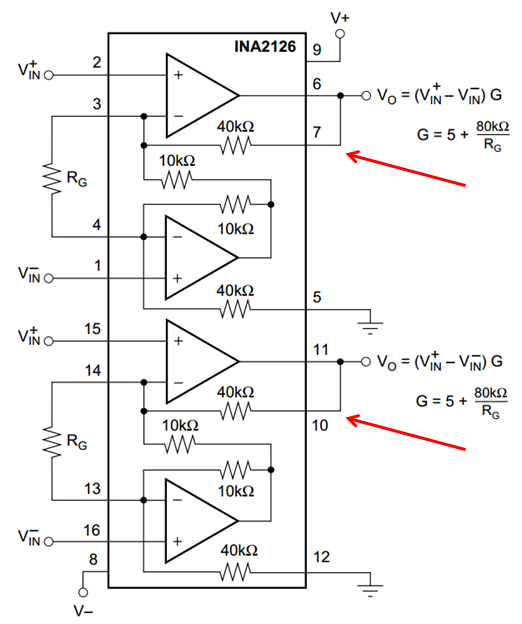
Forum Post: RE: Sense pin in INA2126
Reza,
The sense pin closes the feedback loop of the IN+ amplifier of each channel, this pin should be connected to the VO pin of each channel (Sense A goes to VOA and Sense B goes to VOB).
↧
Forum Post: RE: INA326 Common-Mode and Differential Mode Limits for G=1 ?
Yes, you understood my question and diagram correctly.The 0 ohm case is for just for a fault in the form of a short, so it looks OK.
Thanks, I am learning alot. I did not know that the models in Tina were faithful enough to answer this sort of DC Transfer question. We have Tina Industrial available.
I still have a tough question though. Given all the specs on the current data sheet, how can I deduce that shorting the inputs to a voltage of 2.050 VDC (Vcm=2.05VDC, Vdm=0)*, will produce some error greater than input offset + output offset.....at G=1? Perhaps this sort of question has to be answered with prototyping and simulations....but I am used to getting a chart of Output Voltage Swing Vs Common Mode Voltage for a variety of gains with a +5.00VDC supply and a specified load on the output so that I get a warning or can immediately accept or reject the amplifier.
*Vcm= 1/2 (V+ + V-)
*Vdm= V+ - V-
↧
Forum Post: RE: INA 163 - single supply
I will see if I can measure the impedance on a DSA, but I see your point. With the right package, you can use either the 211 or the 209 on the same PCB.
Filterpro doesn't crank out ladder filters. It does crank out differential filters with the outputs shorted together. ;-)
(Please visit the site to view this file)
I inserted the tina file. This is just a G-job for myself, so nothing to keep secret. The ladder filter takes more silicon, but it has all the nodes driven, so it is less likely to have problems in real life. I'm showing about half a dB of peaking, probably Q enhanced related.
I have the signal flow graph in svg if you want it, but this is textbook ladder design.
↧
↧
Forum Post: RE: Manual 4-20mA Offset Circuit using RCV420 and XTR110
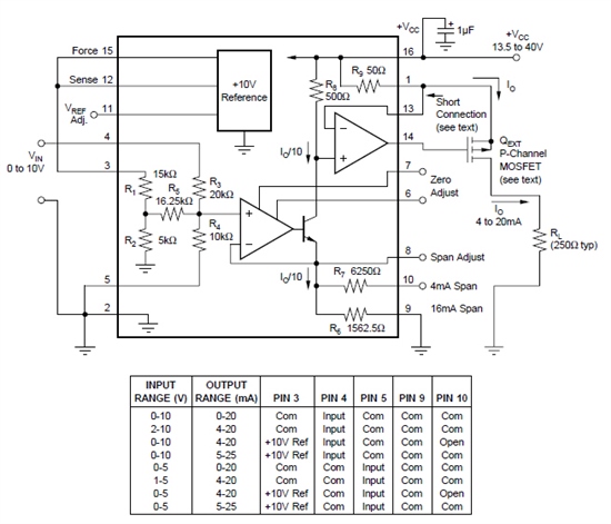
Ok, I am trying to connect a XL-MaxSonar-WR1-MB7052 sensor from MaxBotixInc (which output is voltage from 0 to 5V) to the XTR110 and then the XTR110 to the rcv420 and read this voltage with ADC module of PIC 16F877A from microchip; could you tell me how should I connect the xtr110 and the RCV420 for this purpose?.
↧
Forum Post: RE: Basic RCV420 and XTR110 connections
Hello Omar,
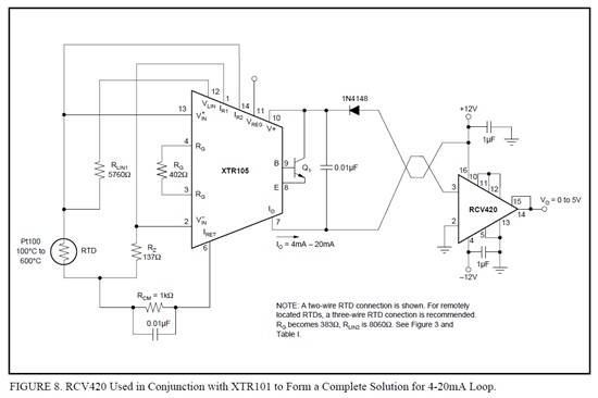
The system you're describing is fairly simple and the basic schematic connections shown in the product datasheets for both devices should suffice to get your system running. I've copied them both below. Configure the XTR110 for 4-20mA output from the 0-5V input as shown in the table below the schematic. Then simply feed the current output of the XTR110 to the RCV420 in place of the XTR105 shown in the 2nd image below. The XTR110 is a 3-wire transmitter so you will send, Power, Signal (IOUT), and GND from the XTR110 to the RCV420 circuit.
Let us know if there are additional questions.
↧
Forum Post: XTR117 Update Rate
Hi,
Customer is going with the XTR117 (2 wire solution) (over the XTR111) and is looking at doing the PWM option like they are showing on page 7 of this datasheet.
In the end they would like to meet or exceed the 12 bit resolution they have today using a DAC and the update rate needs to be 3KHz min.
“I would also like to use the Vreg output as the supply for the isolation...
The trouble I'm having is again at that update rate (3KHz) and ~12 bit resolution on the PWM I need a ~100MHz isolator which requires more current then what can be supplied from the XTR
Does TI have any recommendations for the XTR117 for 3KHz update, small, cheap and uses the Vreg output to power isolation?”
Customer looking at the ISO1541 for isolation.
Any suggestions would be appreciated!
Thanks,
Adam Hoover
ACAT Support
↧